







Different Types of PCBs
Home / Types of PCBs
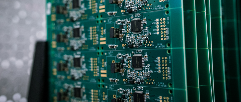
Choosing the right printed circuit board (PCB) for your product is crucial. From single-sided to multi-layer and flexible PCBs, understanding the basics will help you make the best decision.
PCBs are essential components in most electronic devices, providing both physical support and electrical connectivity for components.
PCBs are found in a wide range of industries, including consumer electronics, lighting, media equipment, and aerospace technology. Each type has unique design, manufacturing, and assembly requirements, learn more about the different PCB types and how we can support your project below.
PCBs are essential components in most electronic devices, providing both physical support and electrical connectivity for components.
PCBs are found in a wide range of industries, including consumer electronics, lighting, media equipment, and aerospace technology. Each type has unique design, manufacturing, and assembly requirements, learn more about the different PCB types and how we can support your project below.


Which Type of PCB Do You Need?
Ten common PCB construction types, each suited to different applications. Select any type to see a cross-section diagram and understand where it fits.
Select any PCB type above to see a cross-section diagram and understand its construction, typical applications, and where it fits your project.
Single Sided PCB
Copper on one side only — the simplest construction
Copper on top face only
The simplest and most economical PCB construction, with a single layer of copper on one side of the substrate and no copper on the other. All components and traces exist on the same layer, so any circuit requiring traces to cross paths needs jumper wires or careful layout to avoid it. Single sided boards are typically built on FR4 or, for very low-cost consumer goods, paper-phenolic (FR2) substrate.
Typical use
Simple power supplies, toys
Cost
Lowest of all types
Component limit
~20 components practical
Substrate
FR4 or FR2
Double Sided PCB
Copper on both sides, connected by plated through-holes
Copper both sides, via connects them
Copper is present on both the top and bottom of the substrate, with plated through-holes (vias) providing electrical connection between the two sides. This solves the trace-crossing problem that limits single sided boards, roughly doubling the available routing space. Double sided boards are the workhorse of commercial electronics, handling most designs of moderate complexity without the added cost of multilayer construction.
Typical use
Industrial control, audio
Component count
50–100 comfortably
Layer connection
Plated through-hole vias
Cost
Low to moderate
Multi-layer PCB
Stacked copper layers separated by insulating cores
4, 6, 8+ copper layers with insulation between
Multiple copper layers are laminated together with insulating prepreg between them, typically in configurations of 4, 6, 8, or more layers. Internal layers are usually dedicated ground and power planes, which reduce noise, improve signal integrity, and provide low-inductance return paths. Multilayer construction is needed for high-speed digital signals, RF designs, dense component populations, or where board size is tightly constrained. It's a significant cost step up from double sided but the only viable option once signal integrity or density demands it.
Typical use
Telecoms, computing, medical
Common configs
4, 6, 8, 12+ layers
Key benefit
Signal integrity, density
Cost
Moderate to high
Rigid PCB
Fixed-shape board on a solid FR4 substrate
Solid, non-flexing FR4 construction
The standard PCB construction used across the vast majority of electronic products. Built on a solid FR4 fibreglass-epoxy substrate that holds a fixed shape and provides mechanical support for components, connectors, and mounting hardware. Rigid boards can be single, double, or multi-layer, and this term simply distinguishes them from flexible or rigid-flex alternatives. Unless a design has a specific need to bend, fold, or fit an unusual enclosure shape, rigid is almost always the right and most economical choice.
Typical use
The default for most products
Substrate
FR4 fibreglass-epoxy
Layer options
Single through multilayer
Cost
Most economical baseline
Flexible PCB
Bends and flexes on a polyimide substrate
Bends around tight spaces and moving parts
Built on a thin, flexible polyimide film rather than rigid FR4, allowing the board to bend, fold, or flex repeatedly without damage. Flexible PCBs are used where space constraints demand a board that conforms to an unusual shape, where the connection needs to move during operation (such as inside a hinge or moving assembly), or to eliminate connectors and cabling by replacing them with a single flexible circuit. They require different design rules than rigid boards, particularly around bend radius and copper ductility.
Typical use
Wearables, cameras, hinges
Substrate
Polyimide film
Key design rule
Minimum bend radius
Cost
Higher than rigid
Rigid-Flex PCB
Rigid sections joined by flexible circuit connections
Best of both — rigid support, flexible link
Combines rigid PCB sections with flexible interconnecting sections in a single, continuously laminated structure. Components mount on the rigid areas, which provide mechanical stability, while the flexible sections allow the assembly to fold into 3D shapes or connect boards that need to move relative to each other. Rigid-flex eliminates the connectors and cables that would otherwise link separate rigid boards, improving reliability and reducing assembly complexity, at a higher unit cost and longer lead time than either rigid or flex alone.
Typical use
Aerospace, medical devices
Key benefit
Eliminates connectors/cables
Complexity
High — specialist process
Cost
Highest of common types
HDI PCB
High Density Interconnect — microvias and fine features
Microvias enable much finer routing density
Uses laser-drilled microvias, finer trace and space geometries, and sequential lamination to achieve much higher routing density than conventional PCB construction. HDI is the enabling technology behind modern smartphones, wearables, and any product cramming dense, fine-pitch components — including BGAs with tight ball pitches — into a small footprint. Microvias, being far smaller than mechanically drilled through-holes, allow far more interconnections per unit area, though at a notable cost premium over standard multilayer construction.
Typical use
Smartphones, wearables
Via type
Laser-drilled microvias
Min feature
<0.1 mm trace/space
Cost
Premium over standard multilayer
LED / Metal Core PCB
Aluminium or copper base for efficient heat dissipation
Metal base draws heat away from the LED
Built on an aluminium or copper metal core rather than standard FR4, with a thin dielectric layer providing electrical insulation between the copper circuit layer and the metal base. The metal core acts as an integrated heatsink, drawing heat away from high-power LEDs far more effectively than FR4 alone could manage. This construction is essential for LED lighting, automotive lighting, and any high-power-density application where thermal management would otherwise limit component lifetime and light output.
Typical use
LED lighting, automotive
Base material
Aluminium or copper
Key benefit
High thermal conductivity
Dielectric
Thin thermal-conductive layer
Blank PCB
Unpopulated bare board, ready for assembly
Manufactured but not yet assembled
A "blank" PCB refers to the finished bare board straight from the manufacturing process, before any components are placed or soldered onto it. It has completed copper etching, drilling, solder mask, surface finish, and legend printing, and has passed electrical test — but carries no components. This is the deliverable a PCB manufacturer supplies to an assembler, or to a customer intending to hand-populate the board themselves for prototyping or repair purposes.
State
Fully manufactured, unpopulated
Typical buyer
Assemblers, hobbyists
Includes
Mask, finish, legend, test
Next step
SMT or hand assembly
Custom PCB
Non-standard shapes, materials, or specifications
Tailored to unusual shape or spec requirements
Covers any PCB falling outside standard rectangular, off-the-shelf specifications: unusual board outlines to fit a specific enclosure, exotic substrate materials for extreme thermal or RF performance, non-standard copper weights, castellated edges for module-to-module mounting, or panels combining multiple different board designs. Custom work typically requires closer collaboration with the manufacturer at the design stage to confirm manufacturability before committing to tooling.
Typical use
Unusual enclosures, RF, modules
Key step
Early DFM review
Materials
Beyond standard FR4
Lead time
Typically longer
Looking for a bespoke manufacturing solution?
See how ABL Circuits can help you today:
Call us now on 01462 894 312
Quick Quote
Complete our detailed form for a more accurate quotation.
Alternatively, for a quick overview, fill out the basic form to the right.
Alternatively, for a quick overview, fill out the basic form to the right.
Thank you! Your submission has been received!
Oops! Something went wrong while submitting the form.
ABL Circuits have offered a state of the art PCB Manufacturing Service for over 40 years.


Get In Touch

ABL Circuits Ltd Icknield Way,
Baldock Hertfordshire, SG7 5BB
United Kingdom


© ABL CIRCUITS 2025