


Multi-Layer PCBs
What is a Multilayer PCB?
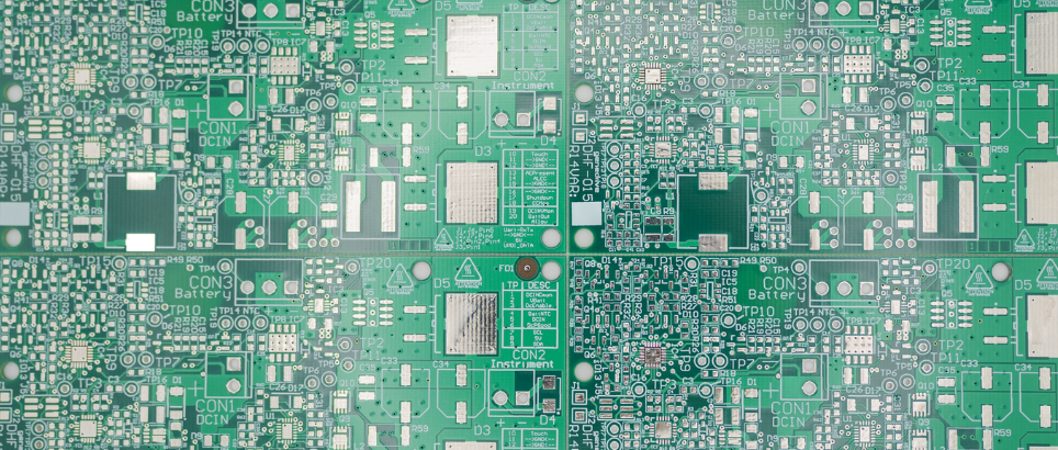
Many printed circuit boards (PCBs) have one or two conductive layers, built on either a single-sided or double-sided substrate. A multilayer PCB, by contrast, is designed and manufactured using multiple layers of base material - typically three or more conductive layers, making it suitable for more complex applications.
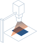
Multilayer PCBs are built using a “sandwich” structure, with multiple double-sided conductive layers separated by insulating material sheets. These layers are bonded and laminated together under high pressure and temperature to eliminate air gaps and ensure the final assembly is durable and reliable.

Are Multilayer PCBs Better Than Double-Sided PCBs?
The answer depends on your application. While multilayer PCBs are generally more expensive to produce, they offer distinct advantages that can be crucial for certain products:
- Improved durability – Additional layers result in a stronger and more robust structure.
- Enhanced quality – The increased design complexity often leads to more meticulous manufacturing.
- Support for complex, high-performance circuits – Multilayer designs can handle the speed, capacity, and power demands of advanced electronics.
- Space-saving – By stacking layers, multilayer PCBs reduce the overall footprint, allowing more compact and lightweight devices.
- Single connection point – Unlike using multiple separate PCBs, a multilayer board typically requires only one power input.
How Are Multilayer PCBs Manufactured and Used?
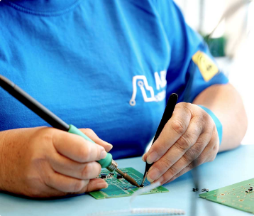
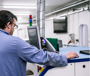
The manufacturing process for multilayer PCBs follows many of the same steps as standard PCB production but includes additional phases for assembling and laminating the complex layered substrate. This ensures the multiple conductive and insulating layers are bonded together securely to deliver a durable, high-performance board.
As specialists in the design and manufacture of multilayer PCBs, ABL Circuits provides advanced solutions across a wide range of industries. Multilayer PCBs are commonly used in:
- Computers and laptops
- Mobile phones and tablets
- Medical equipment
- GPS trackers
- Other sophisticated electronic devices requiring compact, high-functionality designs
Looking for a bespoke manufacturing solution?
See how ABL Circuits can help you today:
Quick Quote
Alternatively, for a quick overview, fill out the basic form to the right.
ABL Circuits have offered a state of the art PCB Manufacturing Service for over 40 years.


ABL Circuits Ltd Icknield Way,
Baldock Hertfordshire, SG7 5BB
United Kingdom


