


PCB Manufacturing

Advanced PCB fabrication from prototype to production. Precision CNC drilling, multilayer lamination, and rigorous testing—delivering high-quality printed circuit boards with fast turnaround times.
ISO 9001-2015 certified. 40+ years UK manufacturing experience.
Our Manufacturing Capabilities
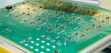
Complete PCB Fabrication
- Single-sided, double-sided, and multilayer PCB manufacture
- Flexible and rigid circuit boards
- Prototype PCB and small batch production
- High-volume manufacturing with consistent quality
- Reverse engineering services
- Small scale PCB manufacturing options available
Advanced Technology
- Precision CNC drilling with laser verification
- Four-head flying probe testing for bare board validation
- Shadow line carbon plating for perfect hole connections
- ISO 9001-2015 certified production control systems
UK PCB Manufacturer
Everything manufactured in-house at our Baldock, Hertfordshire facility. Complete traceability and technical support from our designers and engineers.


The PCB Manufacturing Process
1. Design and Gerber Files
Your PCB design files form the blueprint for fabrication. We accept standard Gerber format and extended Gerber (RS-274X). Our design for manufacture review ensures your design is optimised for the production process.
2. Inner Layer Preparation
Copper foil is laminated onto substrate material. UV light exposure through photo-sensitive film transfers your circuit pattern onto each inner layer. Areas meant to harden receive a blast of UV light, protecting the desired copper traces. Unexposed resist is washed away with an alkaline solution.
3. Etching
Unwanted copper is chemically removed, leaving only your circuit traces. The resist covering the copper is stripped, revealing exposed copper in the exact pattern specified by your PCB design.
4. Layer Alignment and Lamination
For multilayer PCB construction, inner layers are precisely aligned using registration pins. The layers are placed together with prepreg (pre-impregnated laminate) material between each copper layer. Heat and pressure in the laminate press bond everything into a solid board.
5. Precision Drilling
Our CNC drilling system creates holes with micron-level accuracy. The auto-tool change head selects the correct drill bit for each hole diameter, adjusting speeds for optimal precision. Laser verification checks diameter, length, and positional accuracy on every hole drilled.
6. Plating Process
Shadow line plating coats each hole with carbon before the copper plating process begins, guaranteeing perfect electrical connection from one side of the board to the other. Surface finishes include electroless nickel immersion gold (ENIG) for superior solderability when required.
7. Solder Mask Application
Solder mask protects copper traces from oxidation and prevents solder bridges during PCB assembly. This thin layer of protective coating is applied to all outer layers of the PCB, with openings only where components will be soldered.
8. Surface Finish and Silkscreen
Final surface treatment prepares component pads for assembly. Reference designators, component outlines, and other markings are printed onto the board surface for assembly guidance.
9. Testing and Profiling
Every finished PCB undergoes rigorous inspection at multiple process steps. Our four-head flying probe tester validates electrical continuity across all connections. Final profiling cuts boards to exact shape, including complex curved outlines when required.
Quality Control Throughout Production
ISO 9001-2015 Certified
Our production control systems monitor every stage of the board manufacturing process to ensure consistency and reliability across prototype and production runs.
Rigorous Testing
- Flying probe electrical testing on bare boards
- Visual inspection at every production stage
- Dimensional verification to design specifications
- Full traceability from raw materials to finished product
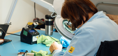
Expert Team
Experienced technicians and engineers guide you through the PCB design process, ensuring your boards meet exact specifications. We can assist with design for manufacture analysis to optimise your PCB for the fabrication process.
PCB Specifications
Thickness Options
Standard: 0.4mm to 1.6mm (0.2mm increments)
Heavy-duty: 2mm, 2.4mm, 3.2mm
Most common: 1.6mm for multilayer boards
Size Range
Smallest manufactured: 5mm square (medical/aerospace applications)
Custom shapes and complex curved outlines available
Panels supplied for assembly when required
Layer Count
Single-sided to complex multilayer configurations
Solder Mask Colours
Green (standard), blue, red, black, white
Copper Weight
Standard through to heavy copper for high-current applications
From Prototype PCB to Production
Fast Prototype Turnaround
Quick validation of your PCB design before committing to production. Small quantities with the same quality standards as full production runs.
Scalable Production
Seamless transition from PCB prototyping to high-volume manufacturing. Our production process ensures every board matches your prototype specifications exactly.
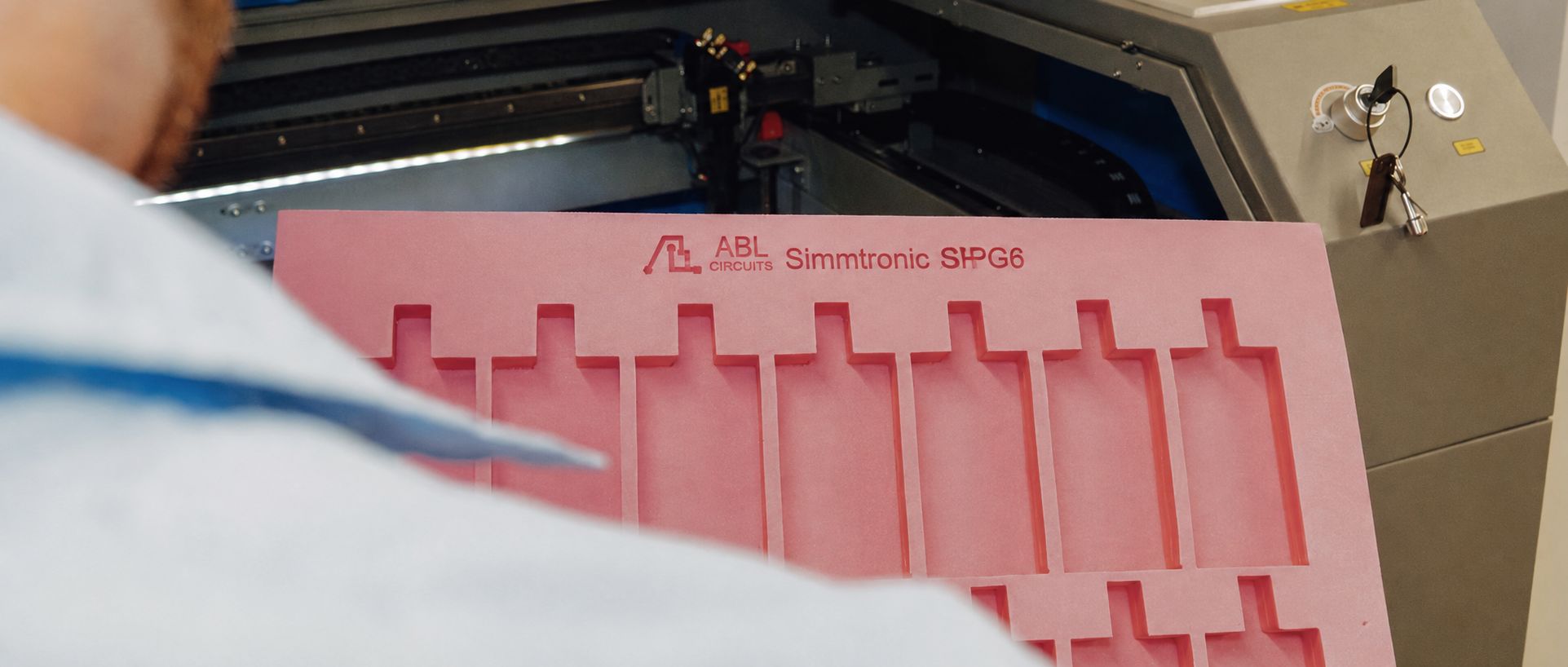
Panelised Boards
PCBs supplied in panel format for automated assembly. Ideal for efficient production and assembly workflows.
Why Choose ABL Circuits?
Complete In-House Control
From PCB fabrication through to assembly—everything under one roof. No outsourcing, complete quality control, faster turnaround times.
UK Manufacturing
Local PCB production with responsive technical support. Fast turnaround without overseas shipping delays. Support British manufacturing.
Design Support
Our team assists with PCB design, design for manufacture analysis, and technical specifications. We help ensure your design is optimised for the manufacturing process before production begins.
Manufacturing Excellence
State-of-the-art equipment combined with decades of experience. Precision results on every board, from prototype to high-volume production.
Competitive Pricing
Direct from manufacturer pricing with no middlemen. UK quality without premium pricing.
Key Differences Between SMT and THT Assembly
PCB assembly uses two main techniques:
Surface Mount Technology (SMT)
SMT components are soldered directly onto the board’s surface, offering:
1
Often using Pick and Place machines.
2
Ideal for compact, high-density designs.
3
Connections may be weaker under stress.
Through-Hole Technology (THT)
THT involves inserting component leads through drilled holes for a stronger connection:
1
Ideal for high-vibration or high-power applications.
2
Additional drilling and soldering steps required.
3
Due to lead-based design and extra material.
Related Case Studies


Can I have my printed circuit boards in a choice of colours?
Can I get my printed circuit boards in different thicknesses?
What is the smallest PCB size I can have?
Can you do complex curved outlines on your printed circuit boards?
Can I have my printed circuit boards left in a panel for assembly?
Looking for a bespoke manufacturing solution?
See how ABL Circuits can help you today:
Quick Quote
Alternatively, for a quick overview, fill out the basic form to the right.
ABL Circuits have offered a state of the art PCB Manufacturing Service for over 40 years.


ABL Circuits Ltd Icknield Way,
Baldock Hertfordshire, SG7 5BB
United Kingdom


