





PCB Design
PCB Design Services
ABL Circuits designs and manufactures your printed circuit boards under one roof at our Baldock, Hertfordshire facility. Because the same team that lays out your board also runs the production line, we design every board to match our own manufacturing tolerances from the start.
That means fewer revisions, fewer manufacturing surprises, and a board that's right the first time.


What You Get
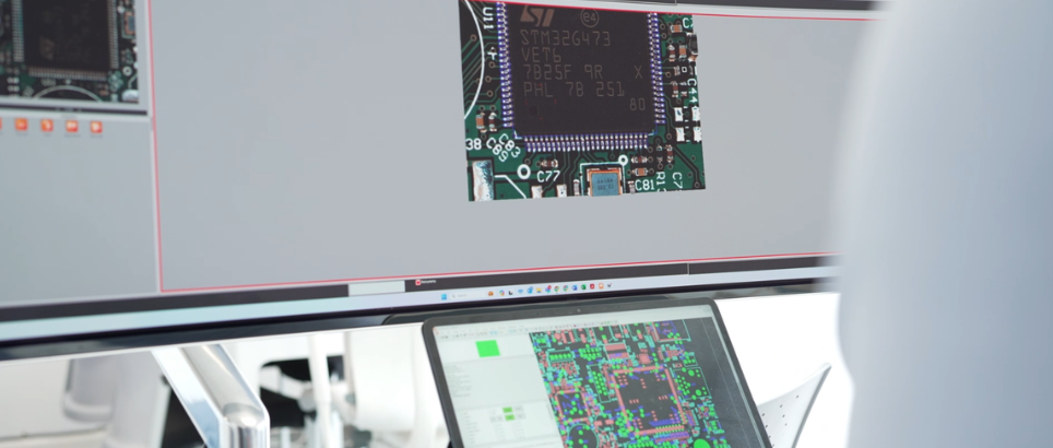
Schematic to layout, handled in-house
Your circuit diagrams and specifications are turned into a manufacturable board layout by our own design team, not outsourced to a third party. Component placement and routing are worked out with our production process in mind, so the design that leaves our design desk is the design that goes straight to manufacturing without rework.
Component placement built for your constraints
Every component from your schematic is positioned to fit your board's real space and thermal requirements. On dense or compact designs this is where most delays happen elsewhere. Because our design and manufacturing teams sit in the same building, placement decisions get checked against production capability before you ever see a final layout.
Routing that matches how we actually build boards
Electrical pathways are routed to suit our own drilling, plating, and soldering processes. This is only possible because design and manufacturing are one team, not two companies working from a spec sheet.
Testing before the board is signed off
Our technicians inspect designs at each stage of manufacturing to catch issues before they reach the final board, rather than relying on design software checks alone.
There's no handover between a design agency and a separate factory, and no shipping delay between design sign-off and the start of production. On past jobs this has let us turn an approved design into bare boards in as little as 5 working days, with urgent orders handled same day.
How ABL Circuits helps with PCB design
At ABL Circuits, we make PCB design straightforward, accurate, and fast. Accuracy is critical, and our experience and attention to detail mean every board meets your specifications right the first time.
Once your design is approved, we can deliver bare PCBs within five working days, and for urgent jobs, same-day PCB manufacturing or rapid PCB prototypes in as little as eight hours are available.
All PCB design is carried out in-house at our Baldock, Hertfordshire facility, keeping design, manufacturing, and assembly under one roof. This complete oversight ensures strict quality control, fast lead times, and consistently reliable boards, giving you confidence in every project from start to finish.
Key Differences Between SMT and THT Assembly
PCB assembly uses two main techniques:
Surface Mount Technology (SMT)
SMT components are soldered directly onto the board’s surface, offering:
1
Often using Pick and Place machines.
2
Ideal for compact, high-density designs.
3
Connections may be weaker under stress.
Through-Hole Technology (THT)
THT involves inserting component leads through drilled holes for a stronger connection:
1
Ideal for high-vibration or high-power applications.
2
Additional drilling and soldering steps required.
3
Due to lead-based design and extra material.
Related Case Studies


How long does PCB design take at ABL Circuits?
Do you handle both the design and the manufacturing?
What information do you need to start a PCB design?
Can you design boards for high-density or space-constrained products?
What if I only need a small batch or a single prototype?
Looking for a bespoke manufacturing solution?
See how ABL Circuits can help you today:
Quick Quote
Alternatively, for a quick overview, fill out the basic form to the right.
ABL Circuits have offered a state of the art PCB Manufacturing Service for over 40 years.


ABL Circuits Ltd Icknield Way,
Baldock Hertfordshire, SG7 5BB
United Kingdom


