







News, Blogs & Articles
What is the SMT process and why should OEMs care?
Case Study
October 7, 2022
Original Equipment Manufacturers (OEMs) are organisations that manufacture or sell products to another company. This company then uses these components in part of a wider process to create products for their customers under their own branding. A big part of creating products to sell on to other companies centres around the SMT process.
What is SMT?
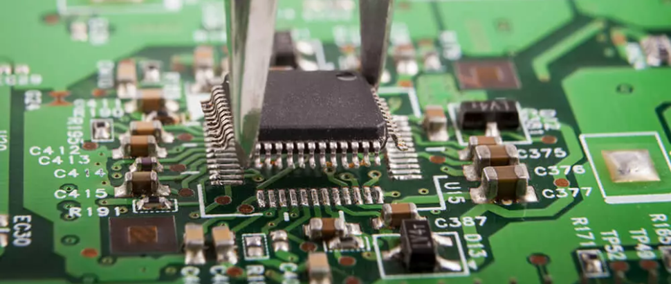
Surface mount technology (SMT) is the process wherein components are mounted onto the surface of a printed circuit board. The components are designed specifically to be directly mounted, rather than hardwired, onto the circuit board for the vast majority of electronics.
Surface mount technology has been widely used since the 1980s. This is because the SMT process is automated, meaning it saves time and costs for both the manufacturer and the customer. Previous methods used hand wiring through holes between the boards to bring components together, meaning this needed manual labour to do so and of course, risked human error. The SMT process is also more adaptable for technological advances in the future than the through hole wire method.
Other advantages of surface mount technology include higher component density and smaller components for mounting alongside better performance under pressure. Using surface mount technology also means that either side of the board can have components mounted on it.
What is the typical SMT process?
There are three main steps to the process when it comes to surface mount technology which cover solder paste printing, component placing and reflow soldering.
Solder paste printing
The solder paste printing process is carried out by a machine to ensure accuracy and speed.
During this part of the assembly, a printer applies solder paste using a pre-made stencil of the PCB and squeegees. This solder paste is usually a mixture of flux and tin and it’s used to connect the SMC and solder pads on the PCB.
During this part of the process, it’s vital that each pad is covered in the correct amount of paste. If not, a connection will not be established when the solder is melted in the reflow oven (more on that later).
Controlling the quality of the solder paste printing process is vital. This is because, if any printing defects are left undetected at this stage, they will lead to other defects further down the line. For this reason, the design of the stencil is key and care must be taken by the assembly team to ensure that the process is repeatable and stable. Thankfully, to smooth the process, most solder paste printers have the option of including an automatic inspection.
However, sometimes external machines are used to assess the quality of the printing. These solder printer inspection machines use 3D technology and allow for a more thorough inspection. This is because they check for things like solder paste volume per pad, rather than just the print area.
Components placement
Once the PCB has passed inspection, it moves to the component placement phase of the SMT assembly process.
During this phase, each component that will be mounted on the PCB is removed from its packaging using a vacuum or a gripper nozzle. Following this, a machine places it in its programmed location. Not only are the machines that carry out this process highly accurate, but they’re also incredibly quick. Some of the most advanced machines can place 80,000 individual components every hour.
When all the individual components have been placed on the PCB, they must be inspected to ensure that they’ve been placed correctly. This is an incredibly important step in the process, because if any placement errors go undetected and the parts are soldered into that position, then this can lead to high volumes of rework, which can be both costly and time-consuming.
Reflow soldering
Once the placed components have passed their inspection, the process moves to the reflow soldering phase. During this part of the SMT process, the PCB is placed into a reflow soldering machine (some people refer to them as reflow ovens).
Here, all the electrical solder connections are formed between the components and the PCB. Using heat, the solder paste applied earlier is converted into a solder. Again, accuracy is vital during this stage of the process because if the PCB is heated to a temperature that’s too high, the parts or assembly could become damaged and the PCB won’t function as intended. If the temperature is too low, a connection may not be established.
To ensure the best results, all PCBs within the soldering machine are placed on a conveyor belt. They’re then heated gradually in a series of zones before being passed through a cooling zone.
To avoid joint defects, the PCBs must stay in each zone for the correct period of time. The PCBs must then also be entirely cooled before they’re handled or moved. If not, they may warp.
After the PCBs have been through the reflow solder machine, they are inspected one final time. This inspection is usually carried out by a 3D automated optical inspection machine (AOI). This is to ensure that the solder joint quality is as expected and that no mistakes have been made during the SMT process. Machines are used for this process because they’re much quicker than humans, and more accurate in their analysis.
How is ABL different?
A tailored service:
ABL Circuits offers a tailored and personal service for all OEMs. We are a one-stop shop for all your PCB manufacturing needs, and can take the entire process from start to end off your hands, or alternatively, assist with an individual aspect along the way.
Family values
We are a family run business which began modestly at our founder, Mark Leverett’s home. Over 40 years on and William Leverett is now director and is helping to run the company with his father. Family is at the heart of everything we do, which means you get a personal and passionate service.
Decades of experience
With over 40 years of experience under our belt, ABL Circuits has a wealth of knowledge across our employees, alongside the newest state of the art technology. As one of the only manufacturers that offer the full start-to-end process, in-house, for PCB assembly, we can help to guide you through every step.
We respect your budget
We work with a range of SMEs and bigger companies and know that it is not ‘one size fits all’ when it comes to budget and delivery. We work closely with each of our customers to understand what they are looking for and how we can provide this in the most cost efficient way, without compromising on quality.
If you’d like to find out more about how we work and how we can help you, get in touch for a quote.
News, Blogs & Articles


.png)
News
How to Write a Design History File (DHF) When Your CEM Is Involved in Development
April 7, 2026
.png)
News
What a Box Build Specification Document Should Include (And What Most Forget)
April 1, 2026
.png)
News
Why JOSCAR Registration Matters When Choosing a Contract Electronics Manufacturer
March 19, 2026
ABL Circuits have offered a state of the art PCB Manufacturing Service for over 40 years.


ABL Circuits Ltd Icknield Way,
Baldock Hertfordshire, SG7 5BB
United Kingdom


