





News, Blogs & Articles
PCB Etching 101
Case Study
March 18, 2022
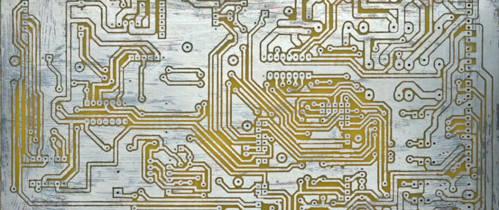
PCB etching is one of the most important elements of the PCB manufacturing process. It involves removing copper from the surface of the PCB in order to reveal the desired circuit pattern.
During the PCB etching process, all copper is removed except for the circuitry that is protected by tin plating. Following this, the tin is then stripped and the copper is cleaned.
Although it sounds straightforward, the PCB etching process is quite complex and precision is vital. Plus, various methods of PCB etching can be employed, and each of these has its own benefits and drawbacks.
To help you understand the PCB etching process in greater detail, we’ve put together this guide. As well as covering what PCB etching is and where it sits within the PCB manufacturing process, we’ve also outlined how we etch PCBs and how we can help meet your needs.
What is PCB etching?
PCB etching is the process of removing unwanted copper from a printed circuit board. Once all of the excess copper has been removed from the PCB, only the required circuit remains.
Before the etching process begins, a layout for the board is generated. This desired layout for the board is transferred onto a PCB by a process called photolithography. This forms the blueprint that decides which pieces of copper must be removed from the board.
On the outer layer of the PCB, the tin plating acts as the etch resist. However, in the inner layer, the photoresist is the etch resist. Generally speaking, there are two approaches to inner layer and outer layer PCB etching. These are dry etching and wet etching. Here at ABL Circuits, we use a wet etching process using a Tech Win Alkali Etching Machine.
Dry etching
The dry etching process usually uses plasma that activates chemical reactions between base and surface atoms of the laminate. This causes the unwanted copper to dissolve. However, although plasma is often used for dry etching, it’s also possible to use lasers for this process.
Plasma etching
Plasma etching has been around since the 1960s. However, it didn’t gain prominence until the 1970s. The process was created as a way to help reduce liquid waste disposal in manufacturing and achieve selectivities that were difficult to obtain with wet chemistry.
With plasma etching, a high-speed stream of glow discharge (plasma) of an appropriate gas mixture is pointed at the PCB. As a result, plasma etching is a dry and clean process that doesn’t require any chemicals.
On top of this, plasma etching is capable of controlled and precise etching at very small scales. It’s also particularly popular because it lessens the likelihood that vias will become contaminated or solvents will be absorbed.
However, although it has its advantages, plasma etching is incredibly costly. As a result, unless you’re etching in vast quantities regularly, it’s likely to be much more expensive than a wet etching method.
Laser etching
The laser etching process allows for the use of precise, computer-controlled hardware. During the process, a high-powered laser carves out trace lines on the PCB’s substrate. These unwanted copper traces either evaporate entirely or are flaked off the PCB.
One of the main benefits of laser etching is that it minimises the number of steps in the process. It also eliminates the need for any inks, acids or toxic chemicals to be used.
However, it can be hard to etch evenly on large boards, and etchant and residues can be hard to dispose of if they don't evaporate entirely. On top of this, as with plasma etching, the laser etching process is very expensive.
Wet etching
The wet etching process uses a solution that dissolves unwanted copper using chemical reactions. Depending on the etch material, either an acidic chemical or an alkaline chemical can be used for this process.
Acidic etching
The acidic method is usually used to etch off the inner layers of a rigid PCB. For this process, either cupric chloride or ferric chloride is used. Of the two solutions, cupric chloride is most common because it accurately etches off smaller features and provides a constant etch rate and continuous regeneration.
Generally speaking, the acidic method is used for the inner layers because the acid doesn’t react with the photoresist and doesn’t damage the required part. In addition to this, the undercuts (the lateral erosion of the etched material below the protective tin/lead layer) are also minimised. However, acidic etching can be a lengthy process and it’s much more time consuming than alkaline etching. As a result, it’s not always suitable for large quantities of PCBs.
Alkaline etching
The alkaline method is commonly used to etch off the outer layers of a PCB. It’s also the method we use here at ABL Circuits.
Alkaline etching is an incredibly fast and cost-effective way of etching a PCB. However, the process must also be closely controlled. This is because the solvent can damage the board if it is in contact for too long.
To make the process as quick, efficient and accurate as possible, alkaline etching is usually carried out in a conveyorised, high-pressure spray chamber. Within the chamber, the PCB is exposed to a refreshed spray of etchant.
During the etching process, the point at which the etching of the unwanted copper is complete is called the breakpoint. This is usually achieved at the midpoint of the spray chamber.
What stage of the manufacturing process is it?
The PCB etching process happens towards the end of the PCB manufacturing process.
After the PCB board has been plated with tin (which helps protect the board), the etching process can begin. Here, etching around the traces is done by passing the board through our conveyorised PCB etching machine, which sprays it with an amonicon edge solution. This removes any surface copper not protected by the tin plating, leaving only the covered tracking remaining on the board’s surface.
Once the board has gone through the PCB etching process, it is dried and fully inspected. Then, it is passed through a tin-stripping machine. This machine uses nitric acid to remove the protective layer of tin over the remaining copper traces.
At this stage, the PCB etching process is complete and the board can continue through the manufacturing process.
How does our PCB etching machine work?
Different forms of PCB etching machines are available on the market. While some PCB etching machines use lasers or plasma to remove any unneeded materials from the PCB, our machine uses an amonicon edge solution.
During the etching phase of the PCB manufacturing process, the PCB is placed on a conveyor belt inside our Tech Win Alkali Etching Machine. Once the machine is switched on, the conveyor belt starts to move and the PCB enters the machine.
When inside, the PCB is sprayed with the amonicon edge solution. This solution then removes all of the copper areas that are not protected by tin. As a result, it only leaves bare fibreglass and the tracks that are protected by the tin coating.
These copper layers are what enable the etched traces – the connective paths – on a finished PCB to carry current and voltage around the board, linking components in a completed circuit.
How can you get started with ABL?
Here at ABL Circuits, we’re one of the UK’s leading printed circuit board manufacturers. Whether you’re searching for manufacturing services, design services or PCB prototypes, we have almost 40 years of experience and we guarantee to meet your needs and requirements. From design right through to assembly, we offer total PCB solutions that you can trust.
Getting started with us is easy. Simply fill in our contact form and a member of our highly-skilled and experienced team will get back to you ASAP.
By partnering with us, you’ll benefit from the fastest lead times in the UK. Plus, we’re always happy to work under strict NDA protocols where requested, and we have built a roster of clients who regularly entrust us with developing proprietary circuits under these conditions.
We pride ourselves on getting the job done right the first time, every time.
News, Blogs & Articles


.png)
News
How to Write a Design History File (DHF) When Your CEM Is Involved in Development
April 7, 2026
.png)
News
What a Box Build Specification Document Should Include (And What Most Forget)
April 1, 2026
.png)
News
Why JOSCAR Registration Matters When Choosing a Contract Electronics Manufacturer
March 19, 2026
ABL Circuits have offered a state of the art PCB Manufacturing Service for over 40 years.


ABL Circuits Ltd Icknield Way,
Baldock Hertfordshire, SG7 5BB
United Kingdom


