


News, Blogs & Articles
Understanding PCB Layer Count: When Do You Need More?
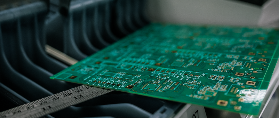
Case Study
October 21, 2025
Choosing the right number of layers for your PCB isn't about showing off technical prowess, it's about matching your design requirements to the most cost-effective solution. Too few layers and your circuit won't work properly. Too many and you've wasted money on unnecessary complexity.
Single-Layer PCBs: The Basics
Single-layer boards have copper traces on just one side. Components sit on top, leads come through holes, and everything connects on that single copper layer.
When Single-Layer Works
Single-layer PCBs suit straightforward circuits where all connections can route without crossing paths:
- Simple power supplies
- LED lighting controllers
- Basic sensors and switches
- Toys and novelty items
- One-off hobby projects
Real-world example: A basic timer circuit for controlling garden irrigation. A handful of components, a 555 timer IC, a few resistors and capacitors, a relay, all connecting in a simple pattern that doesn't require trace crossovers.
The Limitations
The moment you need traces to cross, single-layer becomes problematic. You're forced to use jumper wires (essentially components that bridge over other traces), which adds assembly cost and reduces reliability. If your circuit has more than about 20 components or any real complexity, you've likely outgrown single-layer.
Double-Layer PCBs: The Workhorse
Double-layer boards feature copper on both sides with plated holes (vias) connecting them. This simple addition solves the crossover problem and opens up significantly more routing options.
When Double-Layer Makes Sense
Most commercial electronics use double-layer boards. They're the sweet spot between capability and cost:
- Industrial control systems
- Audio equipment and amplifiers
- Automotive electronics
- Power conversion circuits
- Consumer appliances
Real-world example: A custom PCB for an industrial motor controller. The top layer handles signal routing between the microcontroller and driver ICs, whilst the bottom layer provides power distribution and return paths. Critical high-current traces run on the bottom where they won't interfere with sensitive signals.
The Sweet Spot
Double-layer handles most designs up to moderate complexity. You can typically fit 50-100 components comfortably, include both digital and analogue sections, and maintain decent signal integrity for most applications.
The limitation appears when you need dedicated power planes, impedance-controlled traces, or have dense component populations with complex routing requirements. For PCB assembly of moderately complex circuits, double-layer remains the most economical choice.
Multi-Layer PCBs: Serious Performance
Multi-layer boards stack multiple copper layers with insulation between them. Common configurations include 4, 6, 8, or even 12+ layers, each serving specific purposes in the overall design.
When You Actually Need Multi-Layer
Don't default to multi-layer because it sounds impressive. You need it when your design requires:
Signal Integrity Requirements:
- High-speed digital signals (>100MHz clock speeds)
- Impedance-controlled traces for RF or high-speed serial communications
- Minimal crosstalk between signal traces
- Reduced electromagnetic interference
Real-world example: A telecommunications circuit board handling gigabit Ethernet. A typical 6-layer stackup might be: Signal - Ground - Signal - Power - Ground - Signal. The ground and power planes provide clean references for impedance control whilst shielding signal layers from each other.
Power Distribution Needs:
- Multiple voltage rails requiring clean, low-impedance distribution
- High current requirements (>5A)
- Noise-sensitive analogue circuits requiring dedicated clean power
- Mixed-signal designs separating digital and analogue power
Real-world example: Medical monitoring equipment combining sensitive analogue front-ends with digital processing. Separate power planes for analogue and digital sections prevent switching noise from corrupting measurements. Learn more about healthcare applications where this matters critically.
Physical Constraints:
- Dense component populations requiring extensive routing
- Size restrictions preventing larger board dimensions
- HDI (High Density Interconnect) requirements with fine-pitch components
Real-world example: Smartphone PCBs cramming dozens of ICs into impossibly small spaces. Every millimetre matters, and multi-layer construction is the only way to route everything whilst maintaining signal integrity.
Common Layer Stackups
4-Layer (Most Common):
Top Signal Layer
Ground Plane
Power Plane
Bottom Signal Layer
This configuration suits most designs requiring better performance than double-layer can provide. The internal planes reduce noise and provide excellent power distribution.
6-Layer (High Performance):
Top Signal Layer
Ground Plane
Signal Layer (internal)
Power Plane
Ground Plane
Bottom Signal Layer
Additional ground plane provides better shielding and allows for more complex routing without sacrificing signal integrity.
8-Layer and Beyond: Used in servers, telecommunications equipment, military and defence applications, and other demanding environments where performance cannot be compromised.
The False Economy of Under-Specifying Layers
Choosing too few layers to save money often backfires spectacularly:
- Performance issues: Noise, crosstalk, and signal integrity problems plague designs with inadequate layer counts. A double-layer board forced to handle high-speed signals might work on the bench but fail intermittently in production.
- Layout time: Spending days wrestling with a 2-layer layout, constantly hitting routing dead-ends, often costs more in engineering time than the price difference for a 4-layer board.
- Reliability problems: Inadequate power distribution or ground return paths cause intermittent failures that are nightmarish to diagnose. These issues often don't appear until production, when they're most expensive to fix.
- Redesign costs: Discovering too late that your design needs more layers means starting over—new layout, new prototypes, delayed schedules, and frustrated stakeholders.
As discussed in ways to reduce PCB manufacturing costs, the goal isn't minimising layer count, it's optimising total project cost whilst meeting performance requirements.
Common Mistakes When Selecting Layer Count
Mistake 1: Copying Without Understanding
"Our competitor uses 6 layers, so we should too." This logic ignores that their design might have different requirements, component choices, or performance targets. Make decisions based on your specific needs, not assumptions about others' designs.
Mistake 2: Ignoring Future Requirements
Designing a 2-layer board because it meets today's needs, whilst knowing that next year's version will need additional features, is short-sighted. Adding layers later means a complete redesign. If you're confident about future expansion, plan for it now—even if some layers remain lightly populated initially.
Mistake 3: Underestimating Power Distribution
Digital designers often focus on signal routing and treat power as an afterthought. Modern ICs with fast switching speeds and low voltages need clean, low-impedance power delivery. A microcontroller drawing 200mA might seem trivial, but if that current spikes from 0 to 200mA in nanoseconds, you need proper power planes to prevent voltage sag and noise.
Mistake 4: Skipping the Prototype Phase
Going straight to production with an untested layer count is risky. PCB prototypes let you validate that your chosen layer count actually delivers the required performance. Better to discover problems in 10 prototype boards than 1,000 production units.
Mistake 5: Not Consulting Your Manufacturer
Your PCB manufacturer has seen thousands of designs and knows what works. A quick consultation can identify whether your layer selection will cause manufacturing issues or if there's a better approach you haven't considered.
Making the Right Choice
Use this decision framework:
Choose Single-Layer When:
✓ Circuit has <20 components
✓ No trace crossovers required
✓ Cost is the primary concern
✓ Performance requirements are minimal
✓ You're building a simple one-off project
Choose Double-Layer When:
✓ Moderate component count (20-100 components)
✓ Some complexity but not high-speed signals
✓ Budget constraints matter
✓ Standard performance requirements
✓ Most commercial products that aren't performance-critical
Choose 4-Layer When:
✓ Clock speeds >50MHz
✓ Multiple power rails
✓ Noise-sensitive circuits
✓ Dense component placement
✓ Professional product requiring reliability
Choose 6-Layer or More When:
✓ High-speed digital (>500MHz) ✓ RF or microwave frequencies ✓ Extreme component density ✓ Aerospace, medical, or military applications ✓ Multiple high-current power rails ✓ Impedance-controlled differential pairs
Getting Expert Guidance
Uncertain about the right layer count for your design? This is precisely where working with an experienced PCB manufacturer pays dividends.
At ABL Circuits, we regularly review designs and advise clients on optimal layer counts. Sometimes we recommend adding layers for reliability; other times we identify ways to reduce layers without compromising performance, saving costs.
Our PCB design services include stackup recommendations, power integrity analysis, and signal integrity reviews to ensure your chosen layer count matches your actual requirements.
Whether you're developing proto types or ramping up to production, making the right layer count decision early prevents costly mistakes later. We've seen too many projects derailed by incorrect layer selection—don't let yours be one of them.
Ready to discuss your PCB requirements? Call ABL Circuits on 01443 474 475 or visit www.ablcircuits.co.uk to speak with our technical team about the optimal layer count for your specific application.
News, Blogs & Articles

.png)
News
How to Write a Design History File (DHF) When Your CEM Is Involved in Development
April 7, 2026
.png)
News
What a Box Build Specification Document Should Include (And What Most Forget)
April 1, 2026
.png)
News
Why JOSCAR Registration Matters When Choosing a Contract Electronics Manufacturer
March 19, 2026
ABL Circuits have offered a state of the art PCB Manufacturing Service for over 40 years.


ABL Circuits Ltd Icknield Way,
Baldock Hertfordshire, SG7 5BB
United Kingdom


